Research equipment
We have at our disposal state-of-the-art modern research equipment for extensive characterization of various materials. Sample preparation and analysis can take place in a clean room or inside a glovebox chamber with a nitrogen atmosphere, which prevents oxidation of the samples and contact with moisture.
Examples of equipment and its use:
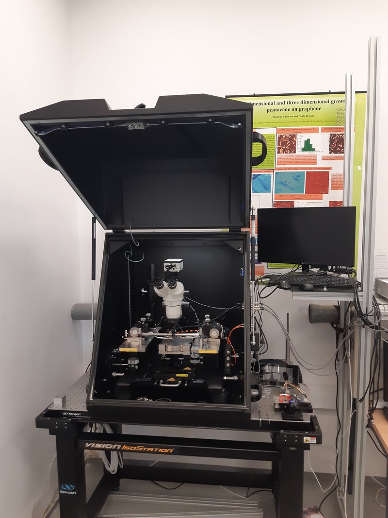
4 point probe station
A station with four probes for measuring the electronic properties of materials with high precision. Possibility to measurement extremely low electric currents. The station is isolated for external vibrations and electromagnetic interference.
Application example: characterization of transistors, electrical semiconductors and solar cells.
Laser lithography
Using a laser to produce finely patterned thin layers on a substrate (eg silicon).
Application example: creation of microstructures and integrated circuits of sizes below 0.0001 millimeter.
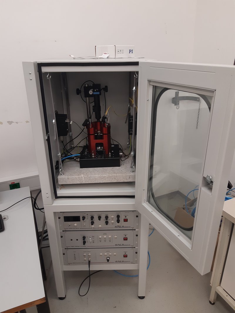
Atomic force microscope
The microscope includes conduction probe and Kelvin probe methods (Bruker CP-II, APE Research A100) and is designed to investigate the surface topography of solid samples with high resolution.
Application example: 2D and 3D topography with atomic resolution, identification of atoms or molecules on a surface and study of their distribution.
Sunlight simulator
Experimental setup for solar cell characterization.
Application example: measuring the efficiency of solar cells under different lighting and atmospheric conditions.
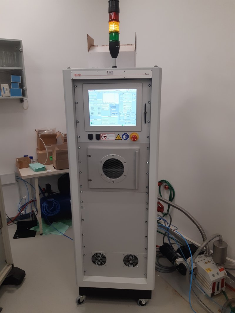
Plasma chamber
Plasma chamber for surface cleaning, sterilization, surface activation and improvement of material properties.
Application examples: improving the performance of solar cells, removing contamination without damaging the sample and using chemicals.
Time-of-flight photoconductivity setup
This method makes it possible to excite charge carriers using a short laser pulse and measure their time of flight. By adjusting the wavelength of the photons, we can also perform a spectroscopic study of the dynamics of photon-to-electron conversion.
Application example: measurement of the mobility of charge carriers in organic semiconductors and 2D materials.